Intel is racing to regain its footing as the unquestioned leader in chip manufacturing technology by 2025.
The Santa Clara, California-based company recently released one of its most ambitious roadmaps in years, full of new process and packaging technologies that Intel argues will close the performance gap with rivals by 2024 and give it process technology leadership by 2025. The goal is to roll out a newer generation of processors—and a new process node to mass-produce it—every year through 2025.
Every generation of processors will be based on more advanced transistors than the last. Intel said that it is bringing features into the fold at every stage of the roadmap, including a new transistor architecture called RibbonFET by 2024 and a new interconnect system called PowerVia the same year. It is also expanding the use of EUV lithography at every node and plans to beat its competitors out of the gate with"high-NA" EUV.
The company revealed the new process and packaging roadmap at its “Intel Accelerated” event last month.
Intel has slipped from the leadership spot in the semiconductor industry in recent years. Behind Intel’s woes is aseries of manufacturing missteps that forced it to delay its most advanced processors for data centers and personal computers. In February, Intel hired its former chief technology officer Pat Gelsinger as CEO to reinvigorate its chip development process and regain ground being surrendered to a growing crowd of rivals.
Because it dragged out the development of its 10-nm node for years, Intel fell behindTSMC in its ability to mass-produce the most advanced chips. TSMC has beaten it to the broader market with its 7-nm node and then jumped ahead to another generation with its 5-nm process, which was first adopted by Apple. TSMC is the world’s largest chip foundry with more than 500 customers, including many of Intel’s leading rivals.
Prolonged delays have opened the door for a growing horde of rivals including AMD and Arm to dent Intel’s dominance in personal computers and data centers. Intel's collapse has raised questions about whether it would expand its use of foundries—or dismantle its manufacturing operations in favor of outsourcing more of its production—to keep it from falling further behind rivals and losing more orders from Apple and AWS.
But Intel doubled down on its manufacturing business with the announcement of its IDM 2.0 strategy, which willsee the Silicon Valley giant keep most of its production in-house and invest tens of billions of dollars in its semiconductor fabs.
One of the pillars of the turnaround plan is expanding its manufacturing operations, starting with $20 billion to build out its U.S. fabs, giving the company the capacity to meet its own needs and mass-produce chips under contract for other firms and even rivals. Intel also formed a foundry business unit, called IFS, and eyeing a ramp-up of its foundry use, including for some of its most advanced processors starting in 2023.
But at the heart of the strategy is anaggressive rebuild of Intel’s manufacturing prowess. "Building on Intel’sunquestioned leadership in advanced packaging, we are accelerating ourinnovation roadmap to ensure we're on a clear path to process performanceleadership by 2025,” Gelsinger said. "We will be relentless in ourpursuit of Moore’s Law."
Intel is also adjusting thenanometer-based node nomenclature that the semiconductor business has used fordecades. The company will rename its process nodes to better align withindustry standards.
Today, the most advanced processorshave up to tens of billions of transistors serving as tiny electronic switchesthat control the flow of current. Every transistor contains a gate mountedon top of the channel that current travels through, bridgingthe "source" and "drain" sides of a channel. A gate is used to control the current traversing the channeland determines whether the transistor is in an “on” or “off” state.
For years, the gate was the mostimportant dimension for determining the performance of a transistor, and thenumber of a process node corresponded to the dimensions of the gate orother parts of the transistor's anatomy. Even though Intel has continued to usenumbered nodes based on the nanometer, the names no longer refer to the lengthor width of the gate or any of the transistor's other internal components.
Today, transistor density is themetric used by experts to compare different nodes. Intel has longargued its process technology can match or beat the performance of nodes numberedthe same way from TSMC and other rivals in terms ofthe density of transistors that can fit on a square of silicon.According to industry analysts, Intel's 10-nm node is roughly on par with TSMC's 7-nm process in transistor density.
Intel said the new node-naming formatwill deliver more clarity to customers, including potential clients of itsfoundry business, and help them understand how the new process technologiesstack up against rival nodes. Ann Kelleher, Intel's SVP oftechnology development, said the new names give more weight to metrics such asperformance, power efficiency, and area while factoring in transistordensity.
The new roadmap runs through the fourtechnology nodes Intel plans to roll out after its 10-nm "SuperFin"node, which is used in its new generation of mobile processors, code named"Tiger Lake," introduced in 2020.

“Intel 7” is what the company plansto call its 10-nm “Enhanced SuperFin” process, which will be used to roll outits “Alder Lake” personal-computer processors in the second half of 2021 and“Sapphire Rapids” CPUs for data centers, which are on pace to be in productionin the first quarter of 2022. Intel improved the FinFET transistors to bring a 10%to 15% boost in performance-per-watt over its previous SuperFin node.
Intel said the “Alder Lake” CPUs arecurrently in mass-production with the Enhanced SuperFin node, which wrings outanother Moore's Law of performance from the 10-nm node to warrant using the “Intel7” name.
"Intel 4" is the technologynode formerly known as the 7-nm process, which Intel was infamously forced todelay out to 2023 due to defects in the production process. The company previouslysaid that its future “Meteor Lake” CPUs would be assembled out of compute tilesbased on the 7-nm node. The node would take full advantage of EUV to imprint smallertransistors on silicon wafers using ultra-short wavelengths of light—and in away that reduces the risk of imperfections that can ruin the final product,improving yields.
Intel said that the node would have 20%more performance-per-watt than its predecessor on the roadmap, as well as area improvements. According to the company, it would be ready by the secondhalf of 2022 so that chips would start shipping in 2023, including its “MeteorLake” CPUs for the personal-computer market and its “Granite Rapids” CPUs for data-centerservers. Test chips are currently in the lab.
“Intel 3” is what Intel previouslycalled its 7-nm+ node, its final technology node based on FinFET transistors.Intel said it would start rolling out chips based on the node by the secondhalf of 2023, delivering around 18% better performance-per-watt. The"Intel 3" node brings more advanced transistor technology into thefold and a high-performance library to assist in area scaling. Intel is alsoexpanding the node’s use of EUV equipment.
Intel is leaning on its 2.5D and 3Dadvanced packaging arsenal to help close its performance gap with rivals. Italso introduced new versions of its Foveros 3D chip-stacking technology set formass-production by 2023.
The final stop on the new roadmap isthe "Intel 20A" node, which the vendor said would open the door tothe "angstrom era" when it is used to manufacture chips in early2024. The "A" in the node stands for "angstrom," or onetenth of a nanometer. Previously known as the 5-nm node, Intel said 20A wouldtake advantage of its RibbonFET and PowerVia technologies to bring it to“parity” with future nodes from TSMC and Samsung.
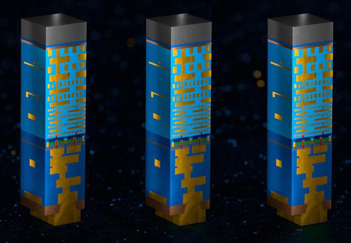
The RibbonFET is Intel’s first newtransistor architecture since it introduced the FinFET a decade ago. A FinFETis formed by applying a fin-shaped flange of silicon to connect the source anddrain sides of the channel in the transistor. The gate—the region thatdetermines whether the transistor is turned on or off—is draped over the fin,surrounding it on three sides. This architecture helps reduce power leakagefrom the transistor. These tiny switches can turn on and off faster and waste lesspower than planar transistors.
The FinFET has been the workhorse inadvanced chips for the last decade of Moore’s Law. The RibbonFETand other gate-all-around transistors promise to cram more performance in a smaller area without sending power requirements through the roof. In RibbonFETs,the fin is flipped on its side so that the gate surrounds the ribbon-shapedchannel on all sides, preventing additional power from leaking out. Intel said these types of transistors offer faster switching speeds at the same drive current asmultiple fins in a smaller footprint.
Intel said PowerVia is the first “backside power delivery” system. Today, themost advanced logic chips contain billions of transistors covered by a layeredcanopy of interconnects of varying dimensions that supply signals and deliver powerbetween them. The interconnects are formed by carving tiny trenches out of a wafer,coating them with cobalt and other metals, and plugging them in with copperwires.
The problem Intel is trying toaddress with PowerVia is that the wires relaying signals and power are tangled together in the same stack of interconnects. But with PowerViatechnology, the wires sending power around the chip are placed behind thetransistors on the backside of the wafer. Thus, power can now be delivered directly tothe transistors rather than traveling a longer distance through floors and floorsof interconnects.
By relocating these wires to theother side of the wafer, the PowerVia technology frees the wires on the frontside of the wafer for improved signal routing. The results are better powerefficiency and higher frequencies.
The semiconductor giant is also earlyin the development on the “18A” process node, which is targetedfor production in the first half of 2025. Intel said that it plans toimprove the RibbonFET transistors at the heart of the process node, resultingin another major leap in performance. Intel said the 18A node is on pace to bemore advanced than future nodes from TSMC, returning it toprocess technology leadership.
Intel has also partnered withsemiconductor gear vendor ASML on the development of new high-numericalaperture (NA) EUV tools that can scorch smaller transistors into chips faster andmore efficiently than the EUV technology in use today. Intel said that itexpects to get the first production high-NA EUV tool in the industry and use iton its production lines by 2025 or later.
Despite the ambitious pace of its newprocess technology roadmap, Intel is playing catch up. TSMC has startedsupplying chips based on its 5-nm technology, while some customers are early indevelopment with chips based on its 3-nm node. That means AMD, Nvidia, Qualcomm,Xilinx, and other chip companies can continue ordering chips that are moreadvanced than Intel’s—and they should be able to for at least three more years.
Obviously, as chip-making become moreexpensive and technologically tough, Intel's new roadmap is not guaranteed.
But the technology industry is notcounting out Intel yet. The company said that it has landed Qualcomm as itsfirst foundry customer for the 20A node due out in 2024. It also announced thatAmazon AWS has agreed to adopt the advanced packaging technology Intel plans toopen to customers of its new made-to-order chip business.


